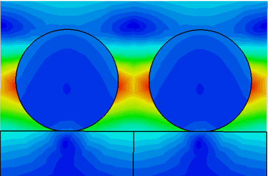
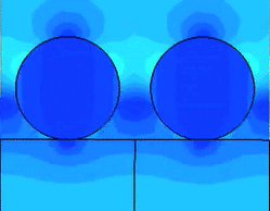
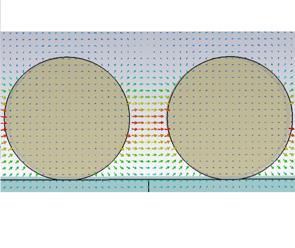
Near-field resonance intensity for the simulated nanostructured solar-cell concept.
Executive summary
- Goal: improve absorption via nanostructure-driven light trapping
- Method: optical simulation of near-field + spectral response
- Focus: resonance behavior and geometry sensitivity
- Outcome: spacing trends that inform efficiency optimization
What was evaluated
- E-field intensity: resonance localization and enhancement
- E-field vectors: energy flow and mode behavior
- Spectral response: dependence on nanowire spacing (horizontal/vertical)
- Design insight: parameters that shift/strengthen resonances
Overview
Nanostructured solar-cell concepts can boost energy conversion by reducing reflection and increasing the optical path length inside the absorber. In this study, we investigated a nanowire-based architecture and quantified how geometry impacts resonance formation, near-field enhancement, and spectral response—key levers for light trapping and absorption improvement.
Why this matters: Even modest absorption improvements can translate into meaningful efficiency gains. Simulations help identify which geometric parameters create strong, broadband-friendly light trapping before fabrication.
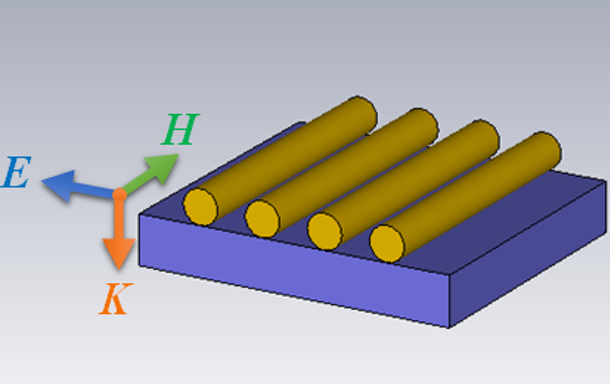
Structure and concept
The simulated structure uses a nanostructure array on a dielectric substrate to manipulate light–matter interaction. Geometry and spacing play a central role in shaping resonance strength, bandwidth, and spectral placement.
Near-field resonance behavior
We analyzed the electric-field intensity and vector patterns at resonance to understand where energy concentrates and how the resonant mode couples into the structure. This helps distinguish between designs that simply shift a peak and designs that create stronger, more useful field enhancement.
Spectral response trends
Spectral results show how nanowire spacing changes the optical response. By sweeping spacing parameters, we can map trends that guide design tradeoffs—such as placing resonances where they most effectively improve absorption while minimizing reflection losses.
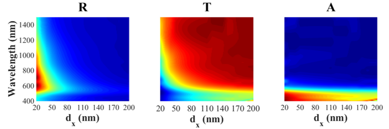
Spectrum of the structure versus horizontal distance (spacing) of nanowires.
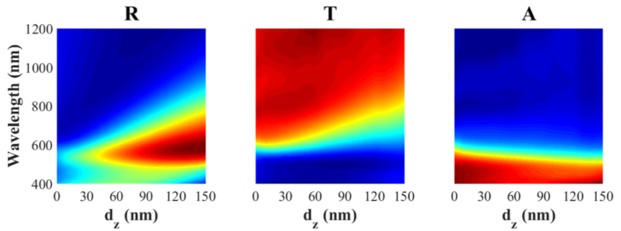
Optical response of the two-layer structure versus vertical distance of nanowires.
Engineering insights
- Enhanced light trapping: nanostructures increase optical path length and can reduce reflection losses through resonant coupling.
- Disordered advantages: non-periodic/disordered arrangements can broaden response and reduce narrow spectral sensitivity compared with highly periodic designs.
- Geometry-driven tuning: spacing and feature size shift resonance location and change field localization—useful for targeting absorber bands.
- Optimization readiness: simulation sweeps identify which parameters yield the largest absorption benefit per manufacturing tolerance.
- Scalability potential: nanostructured concepts may be compatible with scalable fabrication, supporting cost-aware energy applications.
- Design flexibility: material and architectural variants can be explored rapidly once validated trends are established.
Recommendations and next steps
Technical next steps
- Expand parametric sweeps (spacing, height, diameter) to map robust operating regions.
- Track absorption (not only reflection) and compute integrated metrics over the solar spectrum.
- Include realistic material dispersion and loss models for fabrication-aligned predictions.
Engineering validation
- Check tolerance sensitivity to confirm manufacturable design windows.
- Evaluate thermal and reliability impacts if plasmonic/heating effects are expected.
- Plan prototype measurements with appropriate optical characterization methods.
Need optical simulation support for nanostructures or solar concepts?
We help teams translate photonic concepts into simulation-verified designs—parametric sweeps, optimization, and performance interpretation. Contact us at info@tetraelements.com .
Note: Results shown are simulation-based and depend on the assumed material models, boundary conditions, and geometry. Final performance can vary with fabrication tolerances, surface roughness, and measurement setup.