
Resonance field intensity visualization from full-wave simulation of the sensing structure.
Executive summary
- Architecture: nanostructure array + dielectric spacer + ground layer
- Mechanism: resonance-driven near-field enhancement
- Primary outputs: E-field intensity / vectors + reflection spectrum
- Tuning knob: dielectric thickness (spectral shift)
Why it’s useful for sensing
- High local fields can improve interaction with analytes near the surface
- Spectral features (peaks/dips) provide a measurable signature
- Geometry/material control enables application-specific tuning
- Integration-ready layered structure compatible with fabrication workflows
Overview
Resonant nanostructures can concentrate electromagnetic energy into subwavelength regions, enabling stronger light–matter interaction at the sensor surface. In this study, we simulate a layered structure where a metallic nanostructure array sits above a conductive ground plane with a dielectric spacer in between. The goal is to evaluate how the structure supports resonance and how that resonance can be tuned for sensing performance.
Design idea: The ground layer suppresses transmission and forces energy to be redistributed into reflection + absorption channels—often creating strong, localized near-fields around the nanostructures.
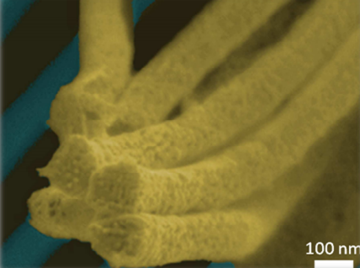
Structure and design intent
The platform uses a three-part stack: (1) metal nanostructure array, (2) dielectric spacer, and (3) metal ground layer. This arrangement supports resonant behavior that can be tailored using geometry and dielectric thickness—useful for placing the resonance at an application-relevant spectral location.

Near-field response at resonance
At resonance, the electromagnetic energy concentrates around the nanostructure features, producing enhanced E-fields and characteristic vector patterns. These near-fields are often the most important driver for sensing performance, because they define the interaction volume near the surface.


Spectral response and tuning
The reflection spectrum provides a measurable signature of resonance. By modifying the dielectric spacer thickness, the resonance location shifts, enabling tunability of the optical response. This is a practical design knob to align the sensor response with target wavelengths or detection bands.

Reflection spectrum of the structure showing resonance tuning by modifying dielectric thickness.
Engineering insights
- Nanostructure array design: geometry and periodicity drive resonance strength and localization.
- Near-field enhancement: resonance concentrates E-fields near the surface—critical for sensing interactions.
- Tunable response: dielectric thickness provides a controllable spectral shift for application alignment.
- Simulation-driven iteration: full-wave modeling enables rapid exploration before fabrication.
- Platform extensibility: the same architecture can be adapted for alternate materials, bands, or integration constraints.
What can be customized
- Nanostructure geometry (shape, width, height, spacing)
- Dielectric material and thickness
- Ground layer material and thickness
- Target resonance location (band placement)
What we typically deliver
- Spectral response (R/T/A) and resonance tracking
- Near-field maps and hotspot interpretation
- Parametric sweeps + optimization recommendations
- Manufacturing-aware guidance (tolerances, layering, integration)
Application areas
- Refractive-index sensing using resonance shifts
- Thin-film / coating characterization via spectral signatures
- Bio/chemical sensing where surface interaction dominates
- Optical filtering / absorber engineering using layered resonance control
Need an optical sensor simulation workflow?
For resonance tuning, parametric optimization, or fabrication-oriented design guidance, contact us at info@tetraelements.com .
Note: Results shown are from full-wave simulation of the presented configuration. Final performance can vary with fabrication tolerances, material dispersion, surface roughness, and measurement setup.